

Quick Facts
- IIT Bombay runs lab-scale 2D semiconductor research at its Nanofabrication Facility, not a commercial foundry.
- A student team, HackerFab IITB, built three chipmaking tools from scratch since August 2025.
- India needs about 30,000 skilled semiconductor workers by 2027, the SemiCon talent committee estimates.
In This Article
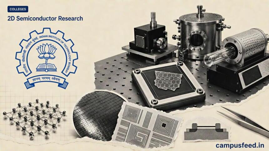
2D semiconductor research at IIT Bombay is building the people and the know-how for India’s chip future, working at lab scale rather than running a mass-production foundry.
The work sits in two places. One is the IIT Bombay Nanofabrication Facility, a research lab where faculty study atom-thin materials like molybdenum disulphide. The other is a student team building chipmaking tools by hand. Together they train the talent India’s fab plans will need.
Key Takeaways
- No sovereign 2D foundry exists in India yet; even global leaders treat 2D chips as early-stage manufacturing.
- IIT Bombay’s real strength is device research plus a growing pipeline of hands-on fabrication talent.
- A student fab shows a college chipmaking setup can be built for roughly Rs 15 Lakh to Rs 20 Lakh.
CampusFeed Take
The honest headline is not that IIT Bombay has built a 2D semiconductor foundry, because it has not, and neither has any country at real production scale. The more useful story for students is that the institute has become India’s clearest example of how chip talent gets made, through frontier device research and a student fab that lets undergraduates touch silicon. Anyone weighing a career in semiconductors should watch the next academic year closely, when IIT Bombay plans to bring undergraduates into hands-on fabrication as part of coursework. That shift, more than any single chip, is what CampusFeed will track. By Harshvardhan Kothari.
What 2D Semiconductor Research Means
A 2D semiconductor is a material only a few atoms thick that can carry and switch electric current. Researchers study these materials because silicon transistors are reaching physical limits as chips shrink. Atom-thin channels may let chipmakers keep improving performance once silicon runs out of room.
The most studied candidate is molybdenum disulphide, or MoS2. Work at the IIT Bombay Nanofabrication Facility has examined how metal contacts behave on MoS2, a core question for making it work as a transistor channel. This is device-level research, the stage where scientists prove a material can function before anyone attempts mass production.
About the IIT Bombay Nanofabrication Facility
The IIT Bombay Nanofabrication Facility (IITBNF) is a shared research lab that grew out of the Centre of Excellence in Nanoelectronics, funded by the Ministry of Electronics and Information Technology between 2006 and 2011. It houses more than 60 faculty members and 15 specialised laboratories. It supports research and training in semiconductor technology and nanotechnology, and users can access its tools through national programmes. You can read its stated mission on the official IITBNF research page.
What IIT Bombay Is Actually Building
IIT Bombay is building research results and skilled people, not a commercial 2D chip factory. The distinction matters because the phrase “foundry” describes a plant that makes chips in volume. What the institute runs is a research nanofab, where the priority is proving new science and training graduate students.
This tradition runs deep. The Department of Electrical Engineering has led microelectronics research in India since 1981, and its first lab fabricated the earliest MOS transistors built at any Indian university. Today the same department is home to a student effort trying to widen who gets to build chips at all. The India Semiconductor Mission, budgeted at Rs 76,000 Crore, has cleared several fabrication and packaging projects, and details sit on the India Semiconductor Mission official site.
Key 2D Semiconductor Milestones and Numbers
The table below sets India’s student-scale work against the global research frontier, so the gap and the opportunity are both clear.
| Milestone | Detail | Source |
|---|---|---|
| HackerFab IITB founded | August 2025, by three IIT Bombay undergraduates | HackerFab IITB |
| Tools built from scratch | Lithography system, sputter, tube furnace | HackerFab IITB |
| Student fab pattern size | 3 to 4 microns, best single demo at 1 micron | HackerFab IITB |
| Global 2D research chip | Around 5,900 MoS2 transistors on one die | IEEE Spectrum |
| Industry 2D milestone | 2D transistors on a 300mm wafer at 50nm pitch | imec, ASML, TSMC |
| India talent need | About 30,000 skilled workers by 2027 | SemiCon talent committee |
The most striking line is the last one. The hardest input to buy is not a machine but a trained person, and that is exactly what the student fab is designed to produce.
The Student Chip Fab Story
HackerFab IITB is a student team that builds low-cost chipmaking tools so undergraduates can learn fabrication by doing it. Founded in August 2025 by Aryamman Bhatia, Abhineet Agarwal, and Kartik U C, the team works from an old photovoltaics lab on campus. In ten months it built three working tools from scratch and fabricated its first simple devices.
Turn Your Achievements Into Stories That Students Actually Read
Feature admissions, placements, rankings, events, research initiatives, achievements, and institutional milestones before a highly engaged education-focused audience.
The team is open about scope. Its lithography system prints features around 3 to 4 microns wide, the resolution of commercial chips from decades ago, not today’s cutting edge. The point is training, not competition. As the team argues, intuition about how a transistor behaves is built by making one, and its tools are cheap enough that a student is allowed to break them. You can follow the project on the HackerFab IITB official site.
“All of that intuition is built at the level of a transistor. That’s why we are trying to be at the level of a transistor,” Aryamman Bhatia told Swarajya.
The bigger claim behind the work is a cost finding. A full student toolkit could be assembled by another college for roughly Rs 15 Lakh to Rs 20 Lakh, the team estimates, comparable to the annual budget of a student racing team. That number reframes chip training as something many Indian colleges could afford, not just the best-funded institutes.
What This Means For You
If you are a student
You do not need to wait for a giant fab to learn chipmaking. A hands-on skill in lithography, deposition, or device testing is rare and valued, and India will need tens of thousands of such workers this decade. Look for semiconductor electives, fabrication labs, and student teams where you can actually build something.
If you are a parent
Semiconductors are a long-term career field with strong government backing in India. A degree that includes real lab work, not only theory, gives your child an edge. Ask colleges whether undergraduates get hands-on access to fabrication or device characterisation, because that experience is what employers increasingly want.
If you run a college or university
A college-scale fabrication setup is now within reach on a modest budget. Open-source tool designs and an active online community mean the barrier is coordination and lab space, not only money. Building such a facility could set your institution apart and plug directly into national chip workforce demand.
If you work in policy or media
The workforce gap, not the machines alone, is the constraint worth tracking. Watch how training capacity scales across colleges, and be precise about the difference between research labs, student fabs, and commercial foundries when reporting on India’s chip push.
What Is Next
The near-term signals to watch are concrete. Keep an eye on these:
- IIT Bombay plans to bring undergraduates into hands-on fabrication through coursework in coming semesters.
- The student team is exploring shared models so other colleges can access fabrication.
- India’s mature-node fabs continue construction, raising demand for trained workers.
If a working student-built transistor and a for-credit fabrication course both arrive on campus, would your college be ready to follow?
Frequently Asked Questions
Last updated: August 28, 2026 at 10:30 IST
Disclaimer: This article is for general informational purposes only and is based on publicly available information at the time of publishing. Programme details, timelines, funding figures, and institutional plans can change without notice. Always verify the latest information from the official portals of IIT Bombay, the India Semiconductor Mission, and the relevant institution before taking any action. CampusFeed and its authors are not responsible for decisions made based on this article. This is not legal, financial, or career advice. Please consult a qualified professional for individual guidance.
Written by Harshvardhan Kothari. Published: August 28, 2026. Updated: August 28, 2026. Have a tip or correction? Write to us at editorial@campusfeed.in.